 Back to list
Semiconductor Industry Network News: Wolfspeed, ROHM, and II-VI have all demonstrated 8-inch silicon carbide substrates in 2015. Among them, Wolfspeed invested 1 billion US dollars to build a new factory and began to produce 8-inch silicon carbide in April this year. Products; Infineon announced in September 2020 that its 8-inch SiC wafer production line has been completed; SiCrystal, a subsidiary of ROHM, expects to start mass production of 8-inch substrates around 2023; Soitec released 8-inch silicon carbide in May 2022 Substrate products, it also launched a new fab construction plan in March 2022.
Domestic and international, the gap on the 8-inch silicon carbide substrate is even more obvious.
The first technical difficulty of the 8-inch silicon carbide substrate is the seed crystal. Although the seed crystal can be made by laser cutting and then splicing, the defect at the splicing position is almost difficult to remove. Basic research on crystal growth can be done. Giving birth will not work. Seed crystals for mass production still need to be expanded slowly. During the expansion process, good quality crystals are retained for optimal reproduction. This process is very time-consuming. Without good seed crystals, it is impossible to reproduce good crystals. Just as good crops cannot grow without good seeds. Usually, the diameter is expanded by a few millimeters at a time, and the expansion time from 6 inches to 8 inches is even in units of years.
Hengpu Technology provides an innovative solution to expand the technical direction of 6 inches to 8 inches at one time, providing a new idea for the industry and promoting the international competitiveness of 8-inch silicon carbide substrates in the domestic industry.
Hengpu Technology uses the angle of ≤45° crystal ingot to grow the crystal with a thickness of ≥30mm, and the unilateral expansion diameter is close to ≥25mm, so that the crystal diameter is expanded by ≥50mm at one time, and the technical route of one-time expansion from 150mm to 200mm is realized.
Hengpu Technology's current unilateral expansion diameter ≥ 20mm, no polytype, microtubes ≤ 0.05ea/cm2, growth rate ≥ 0.3mm/h, no TaC coating on the guide ring;It is expected to reach 25~30mm on one side in the near future Optimize face shape.
Schematic

The core technical difficulties of diameter expansion are: temperature control of thermal field, edge polymorphism, material flow transport (gas phase transport).
Hengpu Technology uses the temperature control technology that has been mastered for many years to adjust the temperature of the thermal field to a temperature gradient that is conducive to crystal diameter expansion, and adjust it.
The gas phase composition is one of the main reasons for the formation of edge polycrystals. Unreasonable gas phase composition is very easy to produce edge polycrystals, which leads to the failure of diameter expansion.
Like crystal growth, material flow is also crucial for diameter expansion. A specially improved [new process] thermal field is used to make gas phase storage and transportation meet the diameter expansion.
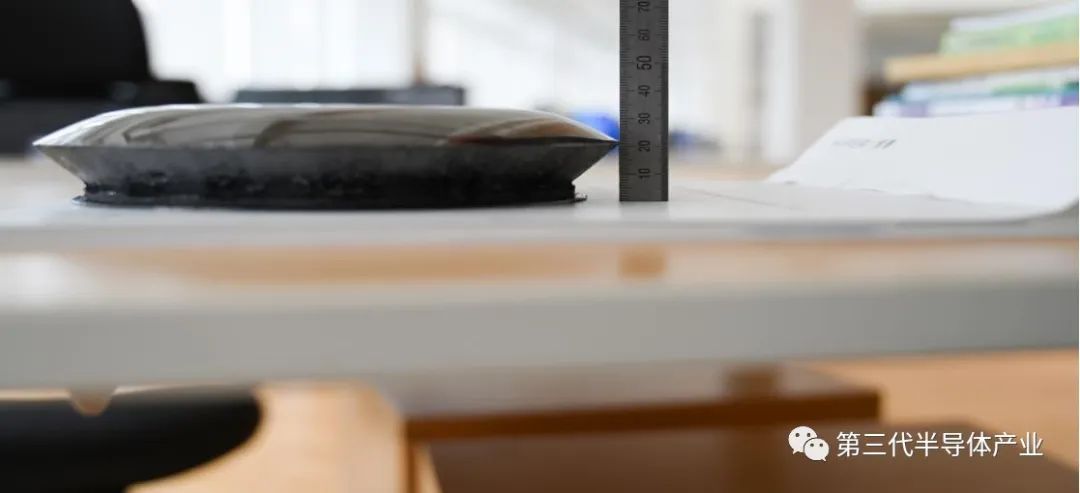
Actual diagram of crystal expansion
Zero laboratory, dedicated to the basic research and innovative direction exploration of materials.
Address:No. 598, Shuangfeng Road, Shuangfeng Industrial Park, Changfeng County, Hefei City, Anhui Province
Tel:0551-6677 0222
Fax:0551-6677 6922
E-Mail:hfroshow@hfroshowsemi.com


Copyright: Roshow Semiconductor Materials Co., LTD. ICP: 2022001243-1 Support:SIXUN