 Back to list
Recommended by the Semiconductor Industry Network: The integration, high frequency and high efficiency requirements of SiCMOSFET devices have put forward higher requirements for the packaging form and process of power modules. This paper summarizes the structural optimization and technological innovation of packaging forms in recent years, including the influence of the length, width and parallel number of metal bonding wires of bonded power modules on parasitic inductance, the effect of direct copper cladding (DBC) on the ceramic layer of the ceramic substrate. The effect of area and height on parasitic capacitance, as well as the use of stacked commutation technology to optimize parasitic parameters, etc.; the influence of the thickness and shape of the buffer layer of the double-sided heat dissipation structure on the heat dissipation index, stress and deformation; summarizes the common failures of power modules The mechanism and solutions provide reference for the safe use of the module. Finally, the requirements and key issues of advanced sintered silver technology are discussed, and the development direction of sintered packaging technology and materials is prospected.
foreword
In recent decades, power semiconductor devices based on the newly developed third-generation wide-bandgap power semiconductor material silicon carbide (SiC) have attracted much attention due to their excellent performance. Compared with the first generation semiconductor materials silicon (Si), germanium (Ge) and the second generation semiconductor materials such as gallium arsenide (GaAs), gallium phosphide (GaP), GaAsAl, GaAsP and other compounds, SiC has a wider band gap. , It has stronger high temperature resistance, higher switching frequency, lower loss and better stability, and is widely used to replace silicon-based materials or applications that are difficult to adapt to silicon-based materials.
(1) Wider forbidden band width: The forbidden band width of SiC is more than 3 times higher than that of Si, so that the breakdown field strength that it can withstand is higher (the critical breakdown field strength is more than 10 times that of Si-based), so the device It can withstand higher peak voltage and output more power. Under the same voltage level, the drift region of the SiC power semiconductor device can be made thinner, which can make the size of the overall power module smaller, and greatly improve the power density of the entire power module. In addition, the on-resistance R on is inversely proportional to the cube of the breakdown field strength, the ability to withstand breakdown field strength is high, and the on-resistance is small, which reduces the conduction loss during the switching process of the device and improves the power module. efficiency.
(2) Higher temperature resistance: It can be widely used in high temperature working conditions with a temperature exceeding 600 °C, while Si-based devices lose their blocking effect due to exceeding their heat resistance capacity when the temperature is around 600 °C. Silicon carbide greatly improves the high temperature resistance of power devices.
(3) Higher thermal conductivity: The thermal conductivity of SiC devices is more than 3 times higher than that of Si. The high thermal conductivity improves the heat dissipation capability of the device and the power module, reduces the requirements for the heat dissipation system, and is conducive to improving the power of the power module. density.
(4) Higher carrier saturation rate: Compared with Si, the carrier saturation rate of SiC is more than 10 times higher, and the switching frequency of SiC devices is 5 to 10 times that of Si-based IGBTs, which enhances the high performance of the device. frequency capability. The SiC device not only has a small on-resistance R on, but also has low switching loss, which improves the high-frequency performance of the power module.
(5) Higher critical displacement capability: Not only the critical displacement capability of SiC is more than 2 times higher than that of Si, but also the stability of SiC devices to radiation is 10-100 times higher than that of Si-based devices, and SiC-based devices have higher resistance to electromagnetic shock and The ability to resist radiation damage. It is suitable for making high-power microwave devices with high temperature resistance and radiation resistance.
However, most of the existing packaging technologies follow the similar packaging of Si-based devices, and there are still many key problems that need to be solved urgently to give full play to the above properties of silicon carbide.
Due to the high frequency characteristics of SiC devices, the junction capacitance is small, the gate charge is low, the switching speed is fast, and the rate of change of voltage and current during the switching process is extremely large. Voltage overshoot and oscillation phenomena cause device voltage stress, increased losses and EMI problems.
Regarding the problems of sharp decline in reliability under extreme conditions such as high temperature and severe cold, it is urgent to find connection materials and packaging processes that adapt to different working conditions and meet the thermal characteristics requirements of different packaging forms.
In view of the problems of internal mutual interference, multi-faceted heat dissipation, large-capacity series and parallel connection, manufacturing cost and difficulty, etc., it is the future trend to appropriately reduce the number of thermal interface layers, reduce module volume, improve power density and multi-functional integration. Adopting advanced heat dissipation technology, pressure sintering process, designing the integration of power semiconductor chips, optimizing multi-chip layout and other methods play a certain key role.
In response to the above problems, domestic and foreign experts and their teams have developed different packaging technologies to improve module performance, reduce stray parameters, and enhance high-temperature reliability.
Wolfspeed Corporation of the United States has developed a high-temperature SiC power module with a junction temperature exceeding 225°C, and reduced the parasitic inductance of the power module to 5 nH. The Global Research Center of GE Corporation in the United States has designed a laminated busbar structure to construct a conduction path that overlaps and parallels the module, reducing the loop inductance to 4.5 nH [7]. German SEMIKRON uses nano-silver sintering and SKiN wiring technology to develop a high-temperature, low-inductance packaging method for SiC power modules. Infineon of Germany has developed high-voltage SiC power modules using crimp connection technology. The Fraunholfer Institute in Germany has developed a high-temperature (200°C), low-inductance (≤1 nH) SiC power module using 3D integration technology. ABB in Switzerland has developed a high-power, low-inductance SiC power module using a 3D packaging layout. Swiss ETH adopts a compact design and optimizes the power loop to develop a low-inductance SiC power module with parasitic inductance ≤1 nH. Nissan of Japan has developed a low-inductance SiC power module based on double-layer direct bonded copper (DBC) packaging, which is used in automotive motor controllers.
The above-mentioned excellent characteristics of silicon carbide can only be fully exerted through the reliability design of the module packaging layout, the selection of packaging materials, the optimization of parameters, the high efficiency of signals and the improvement of packaging technology.
This paper focuses on the summary of key technologies such as low stray parameters, the influence of the buffer layer under the double-sided heat dissipation module, and the failure mechanism of the power module under the typical packaging structure.
1 Module package form
With the development of emerging strategic industries, the demand for the application of the third generation wide bandgap power semiconductor silicon carbide materials and chips, the module packaging technology at home and abroad has also developed rapidly, and the pursuit of low stray parameters and small size packaging technology has become a close link of packaging. Concerns, domestic and foreign scientific research teams and the semiconductor industry have designed high-performance power modules with different structures to improve the performance of SiC-based controllers.
(1) Traditional packaging: Manufacturers such as Wolfspeed, Rohm, and Semikron mostly continue to use traditional Si-based packaging, which has a lower power level, contains metal bonding wires, and has large stray inductance.
(2) DBC+PCB hybrid package: Cha et al. [16] and Seal et al. [17] integrated DBC and PCB board, connected the chip and PCB board through bonding wires, and developed a DBC+PCB hybrid package. The commutation loop is directly controlled between the PCB layers, and the commutation path is reduced to reduce the parasitic inductance.
(3) SKiN package: Germany's Semikron uses nano-silver sintering and SKiN wiring technology, and uses flexible PCB boards to replace bonding wires to achieve electrical connection between the upper and lower surfaces of the chip. The parasitic inductance of the internal loop of the module is only 1.5 nH [18].
(4) Planar interconnect package: By eliminating metal bonding wires, the current loop is extended from the plane layout of the DBC board to the interlayer layout of the upper and lower planes of the chip, which significantly reduces the loop area and stray inductance parameters, such as Silicon Power The company adopts direct terminal connection (DLB) [19], IR's Cu-Clip IGBT [20] and Siemens' SiPLIT technology [21].
(5) Double-sided welding (sintering) package: Weld the DBC heat dissipation substrate on both sides of the power chip to provide heat dissipation channels for the upper and lower surfaces of the chip; or use silver sintering technology to weld DBC on one side of the chip and connect the aluminum sheet on the other side. Double-sided heat dissipation can not only optimize the field strength at the edge of the substrate, but also reduce electromagnetic interference (EMI) and reduce the parasitic capacitance to ground at the midpoint of the bridge arm, which makes it have the advantages of low loss, good thermal performance, and low manufacturing cost. Oak Ridge Laboratory, CRRC Times Electric, Tianjin University and CPES can reduce the parasitic inductance to 5 nH. At the same time, copper sintering as a lower-cost chip connection solution is regarded as a research hotspot in the next few years. At present, the double-sided heat dissipation technology is mainly used in the internal modules of new energy electric vehicles [22−23].
(6) Crimp package: The interface of each layer of the crimp type device relies on pressure contact to achieve electrical and thermal conduction, which is divided into two types: boss-type and spring-type. Compared with solder-type devices, the crimped package structure module has the advantages of high power density, double-sided heat dissipation, low on-state loss, strong shock resistance, failure short-circuit resistance, and easy series connection [24], and uses a small number of pressure The connection type module can meet the voltage level and capacity requirements during commutation [25]. However, due to the sealing and other requirements, the LTCC ceramic design is mostly used, the cost is high, and the crimping packaging structure is complex. Currently, it is only used for the manufacture of high-voltage modules. certain application market. However, there is still a certain gap from the practical application in the automotive field.
(7) Three-dimensional (3D) packaging: Tokuyama et al. [26] and Herbsommer et al. [27] superimposed the upper bridge arm of the SiC module directly on the lower bridge arm. Since the structure of the SiC module is vertical, the commutation loop can be greatly shortened , to further reduce the problems associated with di/d t. At present, the biggest advantage of this packaging technology is that the module parasitic inductance can be reduced to less than 1 nH. In addition, the terminal with the largest voltage fluctuation is placed in the middle of the three-dimensional sandwich structure, which drastically reduces the parasitic capacitance between the terminal and the heat sink [28], thereby suppressing the electromagnetic interference noise [29].
A cross-sectional view of a typical package structure of a power module is shown in Figure 1.

Figure 1 Cross-sectional view of typical package structure
2 Low stray inductance packaging technology
At present, wire bonding is divided into two types: wire and strip. According to different metal properties, there are mainly Al, Cu and Au. Aluminum wire is the most basic bonding method. Aluminum strip has stronger flow capacity and higher strength. Au has relatively few applications due to its high cost. Copper strip is the future trend. Among them, flexible foil, aluminum-coated copper wire and top DBC−copper clip technology also have certain application markets.
For the 3D packaging structure of metal wire-bonded modules, the simulation time of the power module structure can be greatly

Figure 2 Single-sided bonding structure
In this paper, the ANSYSQ3D simulation software is used to extract the parasitic parameters of the model. The length l and diameter d of a single metal bonding wire are used as the parameters to be optimized, and the influence characteristics of l and d on the parasitic inductance are simulated and analyzed, as shown in Figure 3.

Figure 3 Typical 2D packaging structure
The thickness of each layer h1−h7 and the margin a1−a3 are the optimization parameters, where a3 is the distance between the upper copper layer of the DBC structure and the edge of the ceramic layer, because of the insulation performance, DBC pits and solder mask requirements, a3 is generally equal to 1 mm. The specific dimensions of the width w and thickness h of each layer of the traditional typical two-dimensional package structure module are shown in Table 1.
Table 1 Typical dimensions of power modules

For the package structure of metal wire bonding welding, the parasitic inductance mainly comes from the bonding wire, and its parasitic inductance [30] can be approximately expressed as

where l is the length of the bonding wire, l=w1/2+a1; μ0=4 × 10⁻⁷, is the vacuum permeability; d is the diameter of the aluminum bonding wire.
Referring to literature [30], the bonding wire is simulated, and the results are shown in Figure 4. It has been verified that the data fitting results of formula (1) are basically consistent.

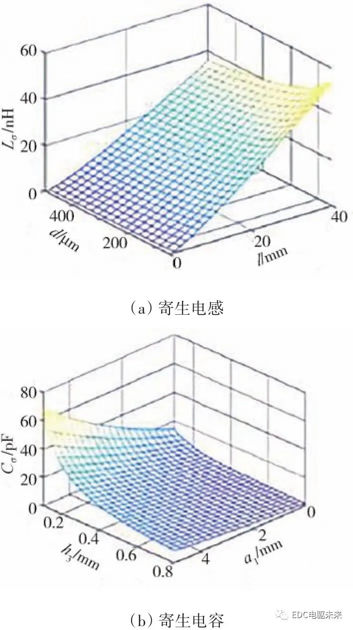
Figure 4 Influence of length, diameter and number of parallel wires on bonding wire inductance
The research of Zeng et al. [31] shows that the parasitic capacitance of the chip power loop is mainly determined by the parasitic capacitance of the DBC ceramic layer, which can be expressed as
In the formula: ε0=8.85 × 10⁻¹² F/m, representing the vacuum dielectric constant; εr=9, representing the relative permittivity of Al2O3 ceramics, for ceramic AIN and ceramic Si3N4, the relative permittivity is equal to 8.8 and 6.7, respectively.
The simulation results of parasitic parameter distribution are shown in Figure 5, which are basically consistent with the data fitting results of equations (1) and (2).

Figure 5 Parasitic parameter distribution
From Figure 4 and Figure 5, it can be clearly seen that each key variable affects the parasitic parameters. The shorter the length of the bonding wire and the larger the diameter, the smaller the parasitic inductance, in which the length of the bonding wire has a more significant effect on the parasitic inductance; the thicker the ceramic layer and the smaller the area, the smaller the parasitic capacitance, and the thickness of the ceramic layer has an effect on the parasitic capacitance more significantly.
Reducing the area of the current flow path in the commutation loop of the switching device can reduce the stray inductance, and the freewheeling diode of the upper half-bridge SiCMOSFET and the SiCMOSFET of the lower half-bridge can be exchanged to reduce the conduction of the commutation path. The area can reduce the stray inductance, as shown in Figure 6, and the simulation results are shown in Figure 7.

Figure 6 Schematic diagram of the commutation path of traditional packaging and stacked packaging

Fig.7 Simulation results of stray inductance of different commutation loops in stacked package
Import the package model of the power module into the stray parameter extraction software ANSYS.Q3D, take the steps of network segmentation and working condition definition in turn, set the excitation source (Source) and ground (Sink), and add the excitation source to the power module terminals respectively. Note that multiple excitation sources can be set, but only one ground can be set. Figure 8 is the meshing diagram of the SiC model.

Figure 8 Stray inductance extraction model and meshing
Niu Ligang et al. [32] showed that the parasitic inductance of the half-bridge power module extracted by ANSYS.Q3D was 20.6 nH, and the actual detection result was 21.23 nH, with a difference of 0.63 nH, that is, the relative error was 3%. The accuracy of the simulation extraction method of dissipated inductance.
The smaller the parasitic inductance of the metal bonding wire, the slighter the parasitic oscillation, the smaller the voltage shock during the switching off process, the higher the switching rate, the smaller the switching loss; at the same time, the parasitic capacitance of the bonding wire should also be as much as possible. small to suppress the effects of electromagnetic interference.
Lσ and Cσ together determine the corner frequency fr of electromagnetic interference (EMI) noise:

3 Double-sided heat dissipation technology
The double-sided heat dissipation power module package structure can reduce the stray inductance, increase the heat dissipation path, and reduce the load on the chip in the power module by eliminating the metal bonding wire, increasing the buffer layer and optimizing the shape, material and size of the buffer layer. long-term high temperature hazards, improve the service life of the module.
According to the number of buffer layers in the double-sided heat dissipation structure, there are three types: no buffer layer, single-layer buffer layer, and double-buffer layer, as shown in Figure 9, wherein the non-buffer layer and the double-layer buffer layer are symmetrical structures. The buffer layer can have different forms, some of which use metal spacers. In the literature [33], the thermal stress distribution of the three modules with the highest junction temperature and the metal spacer structure under the chip heating state was studied.
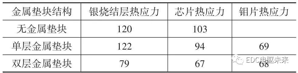
Figure 9 Structure of different buffer layers
The research of Yang Ning et al. [33] found that the thermal stress values of each part of different metal structures are shown in Table 2, and the corresponding simulation cloud diagram is shown in Figure 10. Among them, due to the asymmetry of the structure of the single-layer metal buffer layer, the upper and lower stress layers need to be analyzed separately.

Fig.10 The thermal stress simulation cloud diagram of different buffer layers
Table 2 Thermal stress values of different spacer metal structures MPa
It is not difficult to see from the simulation cloud diagram that the maximum equivalent thermal stress of the double-sided heat dissipation structure without the metal pad buffer layer is 99 MPa; the maximum equivalent thermal stress of the upper substrate of the double-sided heat dissipation structure with a single-layer metal pad buffer layer is 109 MPa, the maximum equivalent thermal stress of the lower substrate is 70 MPa, and the maximum equivalent stress results of the upper and lower substrates are quite different, mainly related to the thermal expansion coefficient and temperature difference between the chip and the metal layer; The effective thermal stress is 81 MPa.
The study by Lu Guoquan et al. [34] showed that with the increase of the thickness of the molybdenum block, the stress buffering effect is obvious and the strain decreases. Both the maximum von Mises stress of the SiC MOSFET chip with double-sided interconnection and the maximum plastic strain of the nano-silver interconnect layer are reduced. At the same time, adding a 1 mm silver spacer in the sintered silver interconnection layer between the buffer layer and the upper substrate can further reduce the chip stress and interconnection layer strain of the double-sided interconnection structure, and improve the thermomechanical reliability of the double-sided heat dissipation SiC module.
Compared with the square buffer layer, the cylindrical buffer layer can effectively eliminate the stress concentration effect of the chip and the nano-silver interconnect layer, and greatly reduce the maximum von Mises stress of the SiC chip and the maximum plastic strain of the sintered silver interconnect layer. When the cylindrical buffer layer is used, the plastic strain of the nano-silver layer is reduced by 47.5% compared with the plastic strain of the nano-silver layer when the square buffer layer is used. This is mainly because the edge of the cylindrical buffer layer is rounded and the stress distribution is more uniform, while the edge or sharp corners of the square buffer layer are likely to cause stress concentration in the chip and the sintered silver interconnect layer, resulting in a sharp increase in local thermal stress.
The double-sided heat dissipation wire-bonded power module is shown in Figure 11. The research of Nakatsu et al. [35] showed that the thermal resistance of the double-sided heat dissipation power module is about 50% smaller than that of the wire-bonded power module; in addition, it also has excellent electrical properties.
Figure 11 Double Sided Thermal Wire Bonded Power Module
The research of Liang et al. [36] showed that the switching loss of a double-sided heat dissipation power module is reduced to 10% of that of a commercial power module. Since the bonding wire will make the parasitic parameter value larger, the parasitic parameter value of the non-bonding wire module is greatly reduced. , the advantages of high temperature resistance and high frequency characteristics of SiC chips have been greatly exerted.
The materials in the module package all have a certain critical thermal stress point, beyond which there is a danger of fracture failure. The substrate size of the SiC power module mainly depends on the area of the chip. The conventional thickness of the insulating substrate is 0.03 mm, and the warpage rate is 3 mil/in. The ceramic material is used as the insulating substrate using direct copper cladding technology. The edge of the metal layer is stepped to effectively reduce the stress, and the height of the step should be half of the copper layer.
The main trend in substrates is to use high-performance materials that reduce the number of layers and interfaces while maintaining electrical, thermal and mechanical properties. Insulated metal substrates (IMS) and IMB substrates are only used for low and medium power modules such as EV/HEV, etc. Mainstream materials are gradually shifting from direct copper cladding (DBC) to active metal brazing (AMB) with high-performance substrates. The double-sided cooling structure will facilitate the use of a 2nd ceramic substrate/lead frame on top of the module.
Directly cooled substrates, such as pin-fin substrates, reduce the number of thermal interfaces and avoid the use of thermal interface materials (TIMs). The integration of substrates and cooling systems along with the deployment of cooling module designs and reducing the number of thermal interfaces will be a strong trend, providing new solutions for years to come. Packaging technology also requires corresponding kits such as ceramic substrates and metal base plates with high temperature reliability [37−38].
Silicone and epoxy materials that can accommodate the higher operating temperatures of silicon carbide equipment are currently under development. In order to achieve complex and compact module designs, in many applications including EV/HEV, silicone is more widely used due to its low price. The application of epoxy resin materials is still limited by the reliability at high temperature.

The failure mechanisms of power modules mainly focus on electrical, temperature, material, chemical and other aspects, as shown in Figure 12.
Figure 12 Failure mechanism of power module
Common damages to power modules include overcurrent damage, overheating damage, and overvoltage damage. Overcurrent damage means that the current flowing through the power module exceeds the current withstand value, and the overcurrent shock causes the chip to generate serious heat, which exceeds the junction temperature withstand temperature value, resulting in damage. chip. The overvoltage damage is that the voltage U GS applied between the drain (G) and source (S) of the SiCMOSFET is greater than the withstand voltage value, which causes the breakdown of the device between the electrodes.
To ensure the safe operation of the power module, it is not only necessary to consider the tolerable range of the current and voltage of the power module, but also to avoid the short-circuit problem of the conduction circuit and the straight-through of the upper and lower bridge arms after the drive signal is added. Therefore, the safe operation of the power module can be guaranteed by adding detection protection circuits and optimizing the control program.
The real failure phenomena of power modules caused by various reasons [39] are shown in Figures 13 to 19. Among them, the short-circuit of the freewheeling diode in the power module and the breakdown and burnout of the collector-emitter are common failure phenomena.

Figure 13 Symptoms of poor soldering

Figure 14 Different effects of ultrasonic wire bonding

Figure 15 Device failure caused by transient overcurrent
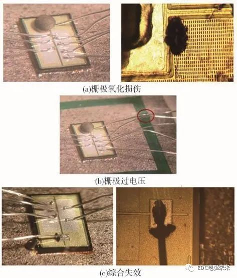
Figure 19 Failure diagram of power module

Figure 16 Chip burnout caused by transient overcurrent

Figure 17 Malfunctions in the glue filling process

Figure 18 Overvoltage breakdown phenomenon of power module
Applying thermally conductive silicone grease evenly as a thermal interface material (TIM) for power modules can no longer meet the requirements. The use of metal sintering and other methods is the next research direction. In addition, adding heat sinks, fans and temperature sensors can effectively prevent overheating problems. Measures such as adding a current transformer detection device and RC snubber circuit and optimizing the program-driven algorithm can effectively solve the overcurrent problem. The overvoltage problem can be effectively solved through bus voltage acquisition and comparison protection.
5 Advanced Technology Outlook
The traditional material process based on welding and wire bonding has unsolvable problems such as low melting point, high temperature creep failure, lead winding, parasitic parameters, etc. New interconnect materials are developing from welding to crimping and sintering technology.
Compared with soldered power modules, the advantages of press-fit modules are as follows.
(1) Welding leads to connect the chip and the PCB board, which is easy to age and fall off after many power cycles, causing the module to fail. Also, solder layer voids increase thermal resistance and reduce reliability. Crimping uses pressure to press the chip on the substrate, and current flows directly from the copper plate to improve reliability.
(2) The traditional welding type is mostly single-sided heat dissipation, while the crimping type is mostly double-sided heat dissipation, which can improve the heat dissipation performance and is conducive to the full performance of the device.
(3) Stray parameters are introduced into the bonding wire and the welding layer. Under high frequency characteristics, the voltage and current are likely to fluctuate greatly, which affects the series characteristics of the chip.
Considering that nano-silver solder paste has high electrical conductivity, high thermal conductivity and excellent ductility, and the melting point is significantly higher than that of traditional solder, the relevant scientific research team used nano-silver solder paste to sinter the chip and the collector molybdenum layer together, and successfully developed a The silver sintered press-fit package shows its advantages in the packaging application of press-fit power modules.
The silver sintered package can reduce the on-voltage and on-state loss of the press-fit device, slow down the contact wear between the chip and the emitter molybdenum layer, and improve the service life of the device.
At present, there are still problems that cannot be ignored in the development of sintered packaging technology, and the following feasible solutions are also proposed.
(1) Due to the problems caused by the different thermal expansion coefficients of silver and SiC chip backside materials, the interconnect performance can be improved by adding a metal buffer layer, but it will increase the complexity and cost of the power module packaging process. Replacing the buffer layer with a sintered layer that meets performance indicators and reliability has become a feasible solution for research and development.
(2) The electromigration phenomenon of the silver layer is not conducive to the long-term reliable application of power electronic devices. Copper sintering satisfies both the reduction of electromigration phenomena and the cost reduction, making it a promising alternative for high temperature die attach materials.
(3) Optimize the sintering industry, innovate the sintering scheme, shorten the preheating and sintering time, and improve the production efficiency; pipeline work, improve the flexibility of manufacturability and production design.
(4) Compared with pressureless sintering, low pressure sintering has better reliability and heat dissipation performance. Although some manufacturers have solved the pressure problem, the problems of densification during sintering, temperature control of the connection layer and performance degradation in extreme environments have yet to be solved.
The solution to the above problems requires the joint and coordinated research of the upstream and downstream of the industrial chain, and some problems will be gradually solved with the advancement of technology. Although the current module packaging is almost entirely based on wire bonding, it is expected that silver sintered packaging technology will be the mainstream technology for power module interconnection in the next 3 to 5 years. Due to the negative impact of silver ion migration on interconnect structures, coupled with cost and thermal stress adaptation requirements, transient liquid phase sintering (TLPS), silver copper sintering, copper sintering techniques and corresponding solder paste materials similar to silver sintering techniques are also rapidly Some technical bottlenecks are expected to break through in recent years. Die attach, substrate connection, module to heat sink connection, etc. are all potential applications of sintering technology.
6 Conclusion
This paper focuses on analyzing and summarizing 4 key issues in the packaging of SiC power modules: (1) Summarizing the packaging forms of low-stray parameter modules with different structures, and enumerating the performance advantages of each module; (2) Focusing on typical packaging structures Next, analyze and summarize the influence of the length, width and number of parallel wires of the metal bonding wire of the bonded power module on the parasitic inductance, the area and height of the ceramic layer in the direct copper cladding (DBC) ceramic substrate on the parasitic capacitance, and the use of lamination (3) In terms of heat dissipation of package modules, the influence of the thickness and shape of the buffer layer of the double-sided heat dissipation structure on heat dissipation and stress deformation is summarized; (4) The common failure maps and solutions of power modules are summarized. Measures to provide reference for the safe use of the module. Finally, the demand and key issues of advanced sintered silver technology are discussed, and the development direction of sintered packaging technology and materials is prospected.
Source: Harbin University of Science and Technology, Cai Wei, Yang Maotong
Address:No. 598, Shuangfeng Road, Shuangfeng Industrial Park, Changfeng County, Hefei City, Anhui Province
Tel:0551-6677 0222
Fax:0551-6677 6922
E-Mail:hfroshow@hfroshowsemi.com


Copyright: Roshow Semiconductor Materials Co., LTD. ICP: 2022001243-1 Support:SIXUN